

Topsil Semiconductor Materials A/S products
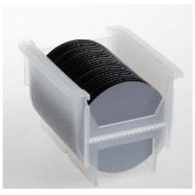
Silicon Wafer Products

Topsil - Model PV-FZ - Photovoltaic Float Zone Monocrystalline Silicon Wafers
Topsil Photo Voltaic Float Zone (PV-FZ™) monocrystalline silicon wafers are recognised for their superior quality in the PV-industry. Float Zonetechnique is used for growing the moncrystals, resulting in wafers with efficiencies above 20%.
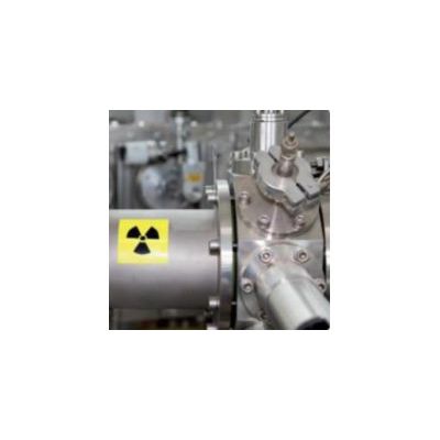
Topsil - Model FZ-NTD - Neutron Transmutation Doped Silicon
Topsil - Model FZ-PFZ - Preferred Float Zone Silicon
Preferred Float Zone (PFZ) silicon can be used for a wide variety of high and medium power applications in which the starting substrate heavily impacts the finished device properties. Preferred monocrystalline silicon has the lowest resistivity variations of the in-situ doped float zone products available and the dopant distribution is tightly controlled throughout the length of the monocrystalline rod.
Topsil - Model FZ-UHPS - Uniform High Purity Silicon for Silicon Drift Detectors
Topsil has designed a unique uniform float zone based high purity silicon substrate (UHPS) with tight resistivity tolerance performing up to unprecedented level. The substrate targets high resolution x-ray, particle and optical detectors. The silicon wafers allow for higher energy resolution and shorter shaping times of detectors used in e.g. space science, crystallography and the medical industry.
Topsil - Model GaN - Float Zone Silicon Wafers
Topsil offers float zone silicon wafers for GaN thin film growth based on a proprietary technology platform and according to customer specifications. The wafers meet various parameters and are available as single sided polished wafers.
Topsil - Model FZ-HPS - High Purity Silicon
Characterised by the highest resistivity range in the market, Topsil Hyper Pure silicon (HPS) is the preferred choice for optoelectronic devices such as infrared detectors, terahertz systems, x-ray mirrors, and silicon lenses, as well as power semiconductors.
Topsil - Model CZ-EPI - Epitaxial Wafers for High Performance Devices
Topsil is a leading supplier of high quality Czochralski based epitaxial (EPI) wafers. The EPI-wafers are used as substrates for low power, medium power and special devices, including schottky, FRED, avalanche diodes, bipolar transistors, Power MOS, IGBTs, MEMS, and ICs. All wafers are customised and meet tight mechanical and electrical parameter specifications according to SEMI standards. They are characterised by tight thickness and resistivity tolerances. Capabilities up to 200mm.
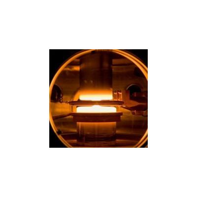
Topsil - Float Zone Silicon (FZ)
Float Zone silicon (FZ) is very pure silicon obtained by vertical zone melting. The process was developed at Bell Labs by Henry Theuerer in 1955.