

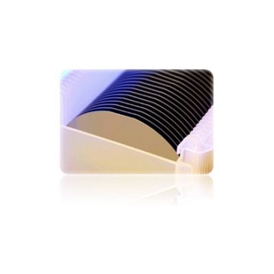
SVM - Double Side Polished Wafers
SVM’s product line includes both single side polished (SSP) and double side polished (DSP) wafer substrates. Double side polished wafers are typically required in semiconductor, MEMS, and other applications where wafers with tightly controlled flatness characteristics are required. They are also needed for double side patterning and device manufacturing projects.
SVM carries a large inventory of double side polished wafers in all wafer diameters ranging from 50mm to 300mm. If your specification is not available in inventory SVM can custom manufacture wafers to your unique specifications. Double Side polished wafers are available in silicon, glass and other materials commonly used in the semiconductor industry.
Below are examples of SVM standard products:
Silicon Wafer
- Diameter: 100mm
- Type/dopant: N or P
- Orientation: <100>
- Resistivity: 0-100 ohm-cm
- Thickness: 525 +/-20um
- TTV: <8um
- STIR: available upon request
- Flats: 1 or 2/ SEMI standard
- Double Side Polished
Silicon Wafer
- Diameter: 200mm
- Type/dopant: N or P
- Orientation: <100>
- Resistivity: 0-100 ohm-cm
- Thickness: 725 +/-20um
- TTV: <5um
- STIR: <2um
- Notch: SEMI standard
- Double Side Polished
All 300mm silicon wafers are double side polished. SVM offers site flatness measurements down to <0.05um or greater, site size 26mmx 8mm, 100% PUA.