

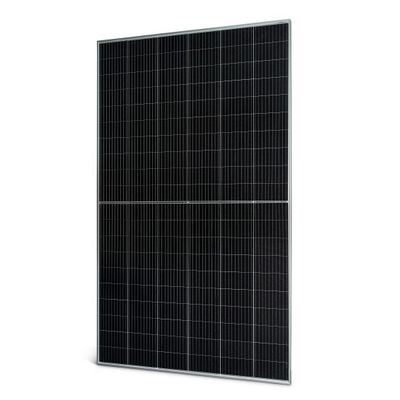
3SUN - Model B60 -Double-sided Modules
High performance
3SUNCORE-H technology converts the highest amount of sunlight in any installation condition.
Guaranteed
Our modules leverage decades of experience by Enel Green Power and ensure maximum reliability and resistance.
European
We manufacture our products in Italy with fully automated processes according to the strictest quality criteria.
A solution that
looks to the future
Our B60 double-sided module was developed using 3SUN CORE-H technology, which has been tested by the industry's leading international investors.
680Wp
of maximum power
thanks to 3SUN CORE-H heterojunction innovative technology.
95%
bifaciality factor
Highest sunlight conversion made possible thanks to a 100% symmetrical solar cell structure.
0%
photoinduced degradation
with total protection technologies against PID, LID and LeTID, and maximum mechanical resistance.
Up to 24%
efficiency
in a 2.172 x 1.303 m format: perfect for large-scale plants.
30 Years
Performance guarantee
max 1% first year degradation, 0.25% yearly degradation for the following years.
-0,24 %/°C
P.Max temperature coefficient
excellent performance even in hot environments and at high operating temperatures.
Zero compromises on quality to secure long lasting products.
Outstanding energy yields
More energy compared to mainstream alternatives.
Bifacial architecture
95% bifaciality factor: the best value on the market.
Minimum energy losses
Extremely low conversion losses caused by overheating and elevated operating temperatures.
Protection over time
No electrical degradation caused by PID, LID or LeTID and market-leading mechanical resistance.
The very best in solar energy conversion and technology development.
3SUN CORE-H technology converts the highest amount of sunlight on both sides of the module, elevating solar energy beyond the limits of the PERC, PERT and TOPCon.
Nothing is left to chance with our solar cells.
TCO - Transparent conductive coating
Innovative transparent and conductive anti-reflection coating, optimized to improve sunlight transmission and convey the generated electrical charges towards the metal conducting grid.
Amorphous silicon (p/n a-Si:H)
P and N amorphous silicon layers applied to maximize the conversion of energy and the conduction of electrical charges by preventing losses and avoiding recombination at the interfaces.
N-type crystalline silicon
Ultra-thin, n-type silicon wafers allow excellent performance and stability while lowering the environmental impact.
Metal conducting grids
Narrow grid multi-busbar technology adopted to minimize resistive losses through improved collection and conduction of electrical charges.
Amorphous silicon (a-Si:H)
Micro-layers deposited to improve output voltage. Using a quantum tunnelling mechanism to create a perfect junction with the crystalline silicon, giving rise to the term “hetero-junction”.