
VIEW Semiconductor Advanced Packaging Applications - Wafer Level Inspection - Electronics and Computers - Semiconductors
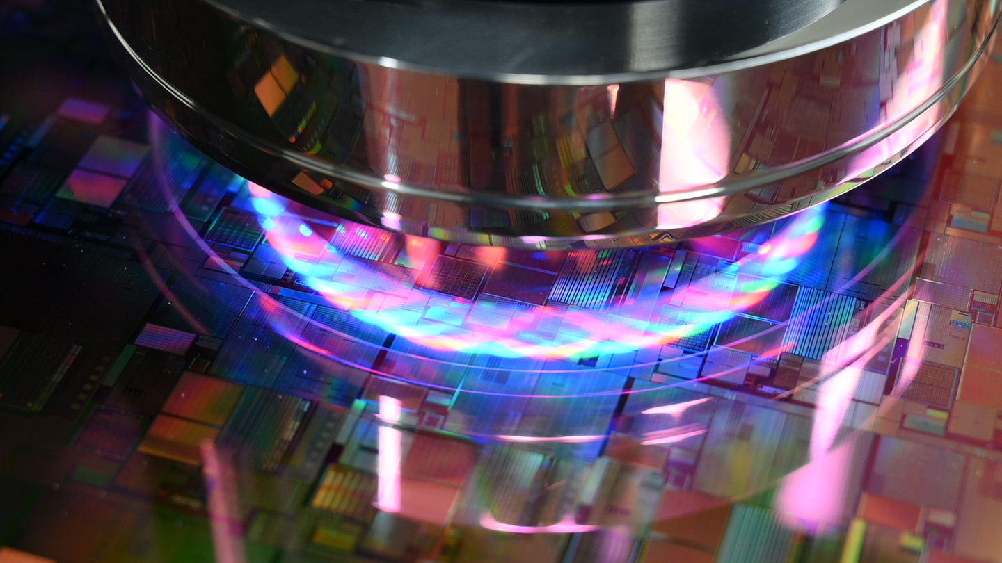
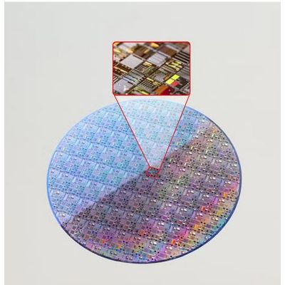
As today’s semiconductor designs continually become smaller and denser, the challenges of wafer inspection are constantly escalating. Extremely small feature sizes can require 50X or higher objective lens magnification and highly programmable top-lighting/back-lighting, along with ultra high-resolution accuracy and repeatability.
Stay in the loop!
Select your areas of interest to receive industry updates.