

- Home
- Companies
- Hiden Analytical Ltd.
- Articles
- Semiconductor Etching Process ...
Semiconductor Etching Process Optimisation via IMP-EPD
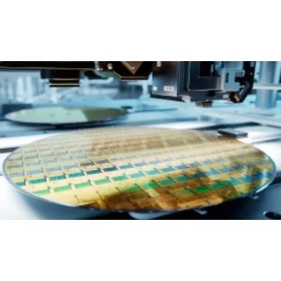
As semiconductor devices shrink to meet the demands of advanced electronics, the precision of material removal during fabrication becomes increasingly important. Processes like ion beam etching must stop precisely at targeted etch depths to preserve layer integrity and device function. In multi-layered device architectures, even minor deviations in etch depth can compromise performance or yield. Achieving consistent, accurate layer removal is therefore a core objective of semiconductor etching process optimisation.
Ascertaining this level of precision requires end point detection (EPD) systems that signal when the etch process has reached or passed through the desired layer. Conventional optical techniques, including interferometry and optical emission spectroscopy, offer some capability but often fail in scenarios involving subtle material contrasts, limited exposed areas, or complex masking patterns. Secondary Ion Mass Spectrometry (SIMS) provides a more effective solution. By analysing the chemical composition of sputtered surface ions in real time, SIMS precisely identifies layers of sub-nanometre thickness. Systems like the IMP-EPD incorporate SIMS directly into the process chamber, delivering immediate, high-sensitivity feedback that strengthens semiconductor etching process optimisation in both research and production environments.
End point detection enables more controlled and data-driven etch process development, particularly when working with unfamiliar materials or introducing new stack designs. Rather than relying on fixed timings, engineers can respond directly to changes in material composition, making recipe refinement faster and more reliable. During production, the ability to detect transitions consistently across wafers supports tighter process windows and reduces the risk of over-etching or layer damage. Such precision is essential in complex, multi-layer architectures where even minimal variation can impact overall device yield and performance.
Secondary Ion Mass Spectrometry (SIMS) provides a precise alternative to optical methods by directly measuring the chemical composition of material removed during etching. A focused ion beam sputters the wafer surface, while secondary ions are analysed in real time to detect different layers of material with sub-nanometre precision.
Effective even under heavy masking and low visibility, SIMS offers reliable compositional feedback crucial for semiconductor etching process optimisation. It also identifies contaminants and trace impurities, supporting process development and production monitoring.
Integrating SIMS into the etch processing tool, the IMP-EPD system continuously monitors wafer composition during etching, enabling immediate control to prevent over-etching and maintain depth precision. This real-time compositional feedback is fundamental to semiconductor etching process optimisation. Additionally, spectral data supports fault analysis and chamber diagnostics, enhancing overall process reliability.
The IMP-EPD system detects secondary ions emitted from the wafer surface during etching, providing real-time, highly precise information about changes in material composition. Its high-resolution detection enables identification of — and end point control within — layers down to 0.5 nanometres in thickness, which is crucial for precise etch control in complex semiconductor structures, directly supporting semiconductor etching process optimisation by ensuring layer integrity and device performance.
Key Features Supporting Semiconductor Etching Process OptimisationHigh-Sensitivity SIMS Detection
Utilises a pulse ion counting detector and a triple-filter quadrupole mass analyser (up to 300 amu) to capture subtle signals from thin layers and small exposed areas, maintaining accuracy even when most of the wafer is masked.
Customisable End Point Algorithms
Integrated Hiden MASsoft software offers:
- Rising and falling ion signal threshold detection
- Layer counting for predefined stack sequences
- Reference peak comparison for improved precision
These capabilities support automated and reproducible end point detection, which is essential for consistent semiconductor etching process optimisation by ensuring each wafer in a batch is processed with uniform accuracy.
Rugged, Production-Ready Design
Engineered for intense production environments, the system includes:
- Differential pumping and protective interlocks
- A Penning vacuum gauge for safe operation
- Compact probe mounting directly on the process chamber for optimal sampling
- Dual functionality as a residual gas analyser for vacuum system diagnostics
Such features enhance equipment reliability and minimise operational disruptions, supporting stable etching processes and consistent manufacturing throughput.
IMP-EPD addresses challenges in advanced materials including:
- Magnetic thin films in memory devices where exact layer integrity is critical.
- High-temperature superconducting layers requiring precise interface detection to maintain functionality.
- III-V compound semiconductors like GaAs and InP with complex multi-layer stacks and subtle compositional variations.
The thin, closely spaced layers and low surface visibility typical of these applications produce difficulties for conventional end point detection methods. The IMP-EPD’s real-time compositional monitoring, with high sensitivity, overcomes limitations in end point detection, reliably identifying end points even under heavy masking or low-contrast conditions. Attaining precise and consistent etch termination reduces defects, improves process stability, and increases overall production yield, strengthening semiconductor etching process optimisation.
Semiconductor etching process optimisation demands precision, accuracy, and reliable monitoring during every stage of fabrication. Systems like the IMP-EPD demonstrate how in-situ SIMS technology can meet such demands by providing sub-nanometre resolution, real-time feedback, and robust hardware integration. Hiden Analytical’s advanced analytical instruments, including the IMP-EPD system, deliver the precise monitoring and control vital for optimising semiconductor etching processes. These tools provide enhanced process insight and reliability, helping manufacturers and researchers achieve higher yields and improved device performance. To see how Hiden Analytical can elevate your semiconductor fabrication, please contact our team today.