
IceMOS Technology Ltd. products
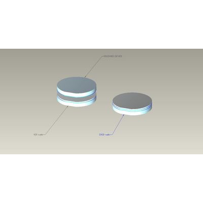
IceMOS - SOI Wafers
ceMOS Technology is a leading supplier of 100-200mm thick-film SOI (Silicon-on-insulator) wafers for a large range of IC and MEMS applications. With over 20 years experience in SOI manufacturing, we offer an impressive specification range, which is amongst the widest available in the market.
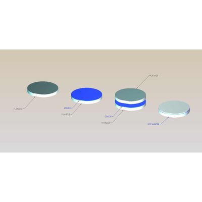
IceMOS - DSOI Wafers
ceMOS Technology is a leading supplier of DSOI for a large range of IC and MEMS applications. With over 20 years experience in SOI manufacturing, we offer an impressive specification range, which is amongst the widest available in the market, ensuring that you receive the perfect DSOI solution for your application. We have extensive experience in SOI substrates and our applications engineering expertise can help you select the best combination of parameters to aid your processing when you get the DSOI wafers.
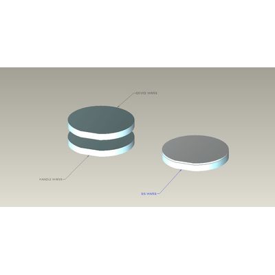
IceMOS - SiSi Wafers
For semiconductor device manufacturers, the IceMOS SiSi bonded wafer offers a cost effective alternative to thick epitaxial layers and inverse epi that have traditionally been used for applications such as power devices and PiN diodes. The use of direct wafer bonding technology allows silicon substrates to be produced containing multiple layers of single crystal silicon. These layers can have a resistivity range 1m?-cm to 10k?-cm., N and P-type and can include combinations of orientations – a feature not possible with conventional epitaxial wafers.
IceMOS - DSP Wafers
ceMOS uses over 20 years of experience to offer the marketplace world class custom DSP solutions (double sided polished). Our highly skilled team has many years of design and manufacturing experience to help develop a DSP solution to your requirement. IceMOS DSP wafers are an excellent substrate for double sided lithography processing; the IceMOS expertise and knowledge of the product and the processes allow for exceptional thickness control. Additionally, non-standard specifications for demanding applications will always be considered.
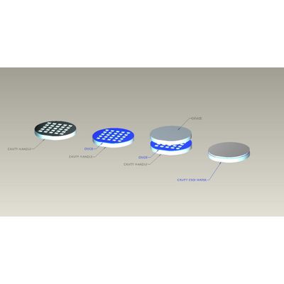
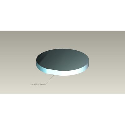
IceMOS - CSOI Wafers
ceMOS Technology is a leading supplier of 100–150mm Cavity Bonded SOI wafers for a large range of MEMS applications. By utilising years of deep silicon trench etch expertise and experience coupled with our advanced wafer bonding technology allow customer cavity expectations to be materialized into innovative products. The IceMOS Cavity Bonded SOI is a pre-etched feature embedded under a silicon membrane. This provides an opportunity for the customer designers to develop more intelligent devices in order to meet the most demanding markets.