

Xiamen Powerway Advanced Material Co.,Ltd products
Gallium Nitride Wafer (GaN)
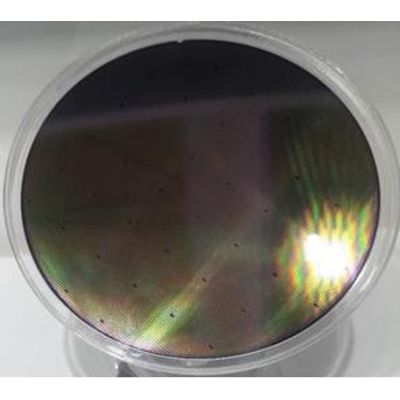
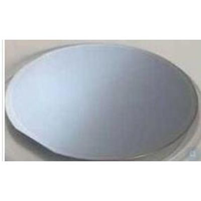
PAM-XIAMEN - Freestanding Gallium Nitride Wafer Substrate
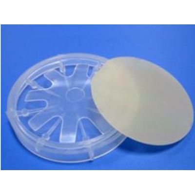
PAM-XIAMEN has established the manufacturing technology for freestanding (gallium nitride)GaN substrate wafer, which is for UHB-LED and LD. Grown by hydride vapour phase epitaxy (HVPE) technology,Our GaN substrate has low defect density.
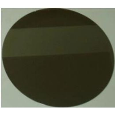
PAM-XIAMEN - Gallium Nitride Wafer Templates
PAM-XIAMEN’s Template Products consist of crystalline layers of (gallium nitride)GaN templates, (aluminum nitride)AlN template,(aluminum gallium nitride) AlGaN templates and (indium gallium nitride) InGaN templates, which are deposited on sapphire.
SiC Wafer
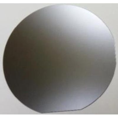
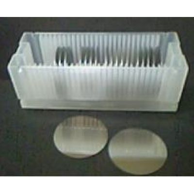
PAM-XIAMEN - Silicon Carbide Wafer Substrate (SIC)
The company has a complete SiC(silicon carbide) wafer substrate production line integrating crystal growth, crystal processing, wafer processing, polishing, cleaning and testing. Nowadays we supply commercial 4H and 6H SiC wafers with semi insulation and conductivity in on-axis or off-axis, available size:5x5mm2,10x10mm2, 2”,3”,4” and 6”, breaking through key technologies such as defect suppression, seed crystal processing and rapid growth, promoting basic research and development related to silicon carbide epitaxy, devices, etc.
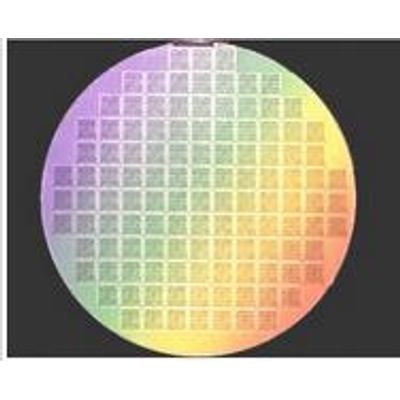
PAM-XIAMEN - Silicon Carbide Epitaxy (SIC)
We provide custom thin film (silicon carbide)SiC epitaxy on 6H or 4H substrates for the development of silicon carbide devices. SiC epi wafer is mainly used for Schottky diodes, metal-oxide semiconductor field-effect transistors, junction field effect
GaAs Wafer
Xiamen Powerway - GaAs Based LD Epitaxy Wafer for Laser Diode
GaAs based LD epitaxy wafer, which can generate stimulate emission, is widely used for fabricating laser diode since the superior GaAs epitaxial wafer properties make the device a low energy consumption, high efficiency, long lifetime and etc. In addition to gallium arsenide LD epi wafer, commonly used semiconductor materials are cadmium sulfide (CdS), indium phosphide (InP), and zinc sulfide (ZnS).
Compound Semiconductor
PAM-XIAMEN - Indium Phosphide Wafer
PAM-XIAMEN offers VGF InP(Indium Phosphide) wafer with prime or test grade including undoped, N type or semi-insulating. The mobility of InP wafer is different in different type, undoped one>=3000cm2/V.s, N type>1000 or 2000cm2V.s(depends on different doping concentration), P type: 60+/-10 or 80+/-10cm2/V.s(depends on different Zn doping concentration), and semi-insulting one>2000cm2/V.s, the EPD of Indium Phosphide is below 500/cm2 normally.
PAM-XIAMEN - Compound Semiconductor Wafer
PAM-XIAMEN offers Compound Semiconductor InAs wafer – indium arsenide wafer which are grown by LEC(Liquid Encapsulated Czochralski) as epi-ready or mechanical grade with n type, p type or semi-insulating in different orientation(111) or (100). In addition, InAs single crystal has high electron mobility and is an ideal material for making Hall devices.
PAM-XIAMEN - Compound Semiconductor Wafer
PAM-XIAMEN offers Compound Semiconductor InSb wafer – Indium antimonide wafer which is grown by LEC(Liquid Encapsulated Czochralski) as epi-ready or mechanical grade with n type, p type or semi-insulating in different orientation(111) or (100). Indium antimonide doped with isoelectronic(such as N doping) can reduce the defect density during the indium antimonide thin films manufacturing process.
PAM-XIAMEN - Compound Semiconductor Wafer
PAM-XIAMEN offers Compound Semiconductor GaSb wafer – gallium antimonide which are grown by LEC(Liquid Encapsulated Czochralski) as epi-ready or mechanical grade with n type, p type or semi-insulating in different orientation(111) or (100).
Germanium Wafer
PAM-XIAMEN - Germanium Single Crystals and Wafers (Ge)
PAM-XIAMEN offers 2”, 3”, 4” and 6” germanium wafer, which is short for Ge wafer grown by VGF / LEC. Lightly doped P and N type Germanium wafer can be also used for Hall effect experiment. At room temperature, crystalline germanium is brittle and has little plasticity. Germanium has semiconductor properties. High-purity germanium is doped with trivalent elements (such as indium, gallium, boron) to obtain P-type germanium semiconductors; and pentavalent elements (such as antimony, arsenic, and phosphorus) are doped to obtain N-type germanium semiconductors. Germanium has good semiconductor properties, such as high electron mobility and high hole mobility.