- Home
- Companies
- Xiamen Powerway Advanced Material ...
- Products
- PAM-XIAMEN - Model InSb - Compound ...
PAM-XIAMEN - Model InSb -Compound Semiconductor Wafer
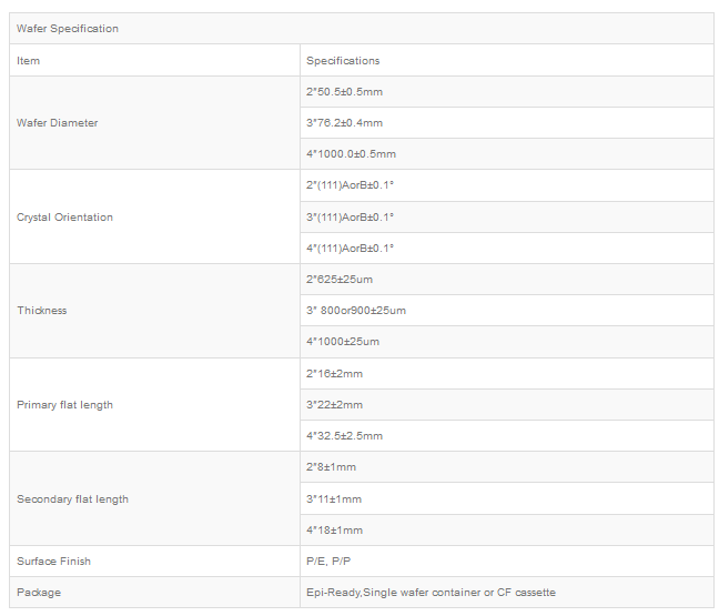
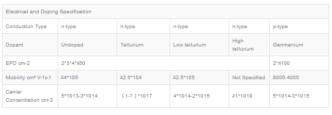
PAM-XIAMEN offers Compound Semiconductor InSb wafer – Indium antimonide wafer which is grown by LEC(Liquid Encapsulated Czochralski) as epi-ready or mechanical grade with n type, p type or semi-insulating in different orientation(111) or (100). Indium antimonide doped with isoelectronic(such as N doping) can reduce the defect density during the indium antimonide thin films manufacturing process.
PAM-XIAMEN offers Compound Semiconductor InSb wafer – Indium antimonide wafer which is grown by LEC(Liquid Encapsulated Czochralski) as epi-ready or mechanical grade with n type, p type or semi-insulating in different orientation(111) or (100). Indium antimonide doped with isoelectronic(such as N doping) can reduce the defect density during the indium antimonide thin films manufacturing process.
Indium antimonide (InSb) is a crystalline compound made from the elements indium (In) and antimony (Sb). It is a narrow-gap semiconductor material from the III-V group used in infrared detectors, including thermal imaging cameras, FLIR systems, infrared homing missile guidance systems, and in infrared astronomy. The indium antimonide detectors are sensitive between 1–5 µm wavelengths. Indium antimonide was a very common detector in the old, single-detector mechanically scanned thermal imaging systems. Another application is as a terahertz radiation source as it is a strong photo-Dember emitter.