- Home
- Companies
- Xiamen Powerway Advanced Material ...
- Products
- PAM-XIAMEN - Model InAs - Compound ...
PAM-XIAMEN - Model InAs -Compound Semiconductor Wafer
PAM-XIAMEN offers Compound Semiconductor InAs wafer – indium arsenide wafer which are grown by LEC(Liquid Encapsulated Czochralski) as epi-ready or mechanical grade with n type, p type or semi-insulating in different orientation(111) or (100). In addition, InAs single crystal has high electron mobility and is an ideal material for making Hall devices.
PAM-XIAMEN offers Compound Semiconductor InAs wafer – indium arsenide wafer which is grown by LEC(Liquid Encapsulated Czochralski) as epi-ready or mechanical grade with n type, p type or semi-insulating in different orientation(111)(100) or (110). In addition, InAs single crystal has high electron mobility and is an ideal material for making Hall devices.
Indium arsenide, InAs, is a semiconductor composed of indium and arsenic. It has the appearance of grey cubic crystals with a melting point of 942 °C and lattice constant of 0.6058nm, and the indidum arsenide crystal structure is a zinc blende structure. Indium arsenide wafer is used for construction of infrared detectors, for the wavelength range of 1–3.8 µm. The detectors are usually photovoltaic photodiodes. Cryogenically cooled detectors have lower noise, but InAs detectors can be used in higher-power applications at room temperature as well. Because of the superior indium arsenide properties, indium arsenide thin films are also used for making of diode lasers.
Indium arsenide band gap is a direct transition, which is similar to gallium arsenide, and the forbidden band width is (300K)0.45eV. Indium arsenide is sometimes used together with indium phosphide. Alloyed with gallium arsenide, it forms indium gallium arsenide – a material with band gap dependent on In/Ga ratio, a method principally similar to alloying indium nitridewith gallium nitride to yield indium gallium nitride.
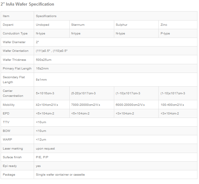
Here is the detail specification:
- 2″(50.8mm)InAs Wafer Specification
- 3″(76.2mm)InAs Wafer Specification
- 4″(100mm)InAs Wafer Specification