
- Home
- Companies
- PCB Technologies Ltd
- Products
- PCB - Model iNPACK - Cutting Edge ...
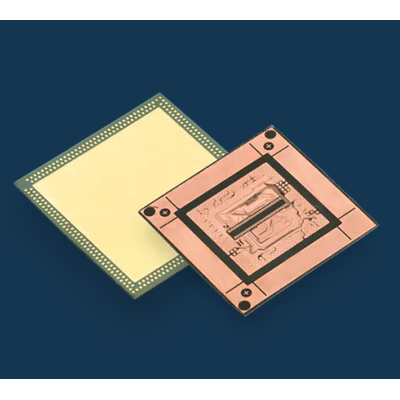
PCB - Model iNPACK -Cutting Edge Semiconductor and Electronics Assembly
We go beyond design limits to offer you cutting edge semiconductor and electronics assembly, testing and IC package design including LGA, BGA and 2D & 3D customized solutions. Featuring fully supported automated processes, MW microelectronics assemblies, System-in-Package (SiP) & heterogeneous integration. We also offer high level expertise in organic substrate design and manufacturing based on advanced materials, subtractive and mSAP processes.
Advanced IC Packaging & Organic Substrates – All-in-One Solutions
We offer organic substrate expertise with high-density line/space width and advanced packaging that allows for a smaller form factor, increased functionality, high thermal conductivity, and improved process stability. System-in-Package (SiP) prototypes, or low/mid volume production, Multi-Chip-Modules (MCM), and more; all compatible with aerospace, defense, medical, and other top industry needs. We specialize in heat dissipation solutions that ensure your projects meet high standards of performance and reliability in the shortest possible time to market.
Organic SubstratesAdvanced Packaging Assembly
Our unique assembly process designs enable you to achieve high-level, customized results with IC packaging solutions tailor-made to your specific applications. Our customers are no longer bound by a specific design process dictated by individual fabricators or semiconductor packaging companies. Instead, we offer you the design freedom to choose from a variety of custom options perfectly aligned with your project needs: Antenna-in-Package, Flip-Chip, QFN package technology, Filter-on-Package, and many more.
Advanced PackagingTechnological Edge
iNPACK are experts in organic substrates and enhanced micro-electronics packaging technologies, with cutting-edge capabilities that deliver complete, comprehensive substrate panel-level manufacturing and engineering support to our customers; in fact, they depend on it. We continuously work to improve interconnections between PCB, Substrate and Semiconductors through advanced technological know-how. Solutions include Organic Substrate materials, IC Substrates, Die Packaging, Multi-Chip-Module (MCM) technology, Chip Packaging and more. Creative solutions and enhanced design flexibility give us the ability to deliver high-speed, thermal and RF pathways that simplify integration processes, that improve overall system reliability. Our common design rules (PCB, Substrate & Packaging) are conveniently located under one roof; providing speedier, high-efficiency services, for your peace of mind.
- IC Packaging & System-in-Package (SiP) design
- Semiconductor assemblies
- MW microelectronic assemblies
- Organic substrates
- Process development & DFM processes
- Time To Market (TTM)
- Design & manufacturing under one roof
- Cost effective solutions
- Innovative approach
- Customization options
- In-house capabilities: substrates, PCB, micro assembly