

- Home
- Companies
- Xiamen Powerway Advanced Material ...
- Products
- PAM-XIAMEN - Freestanding Gallium ...
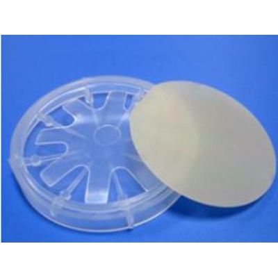
PAM-XIAMEN - Freestanding Gallium Nitride Wafer Substrate
PAM-XIAMEN has established the manufacturing technology for freestanding (gallium nitride)GaN substrate wafer, which is for UHB-LED and LD. Grown by hydride vapour phase epitaxy (HVPE) technology,Our GaN substrate has low defect density.
As a leading GaN substrate supplier, PAM-XIAMEN has established the manufacturing technology for freestanding (Gallium Nitride)GaN substrate wafer which is Bulk GaN substrate for UHB-LED, LD and fabrication as MOS-based devices. Grown by hydride vapour phase epitaxy (HVPE) technology, our GaN substrate for III-nitride devices has low defect density and less or free macro defect density. The GaN substrate thickness is 330~530μm.
In addition to power devices, gallium nitride semiconductor substrates are increasingly used in the manufacture of white light LEDs because the GaN LED substrates provide improved electrical characteristics and their performance exceeds current devices. Moreover, the rapid development of gallium nitride substrate technology has led to the development of high-efficiency GaN free standing substrates with low defect density and free macro defect density. Therefore, such GaN substrates can be increasingly used to white LEDs. As a result, the bulk GaN substrate market is growing rapidly. By the way, bulk GaN wafer can be used for testing vertical power device concepts.
Here shows detail specification: 4″ N type Si doped GaN(Gallium Nitride) Free-standing Substrate
- Item PAM-FS-GaN100-N+
- Conduction Type N type/Si doped
- Size 4″(100)+/-1mm
- Thickness 480+/-50
- Orientation C-axis(0001)+/-0.5o
- Primary Flat Location (10-10)+/-0.5o
- Primary Flat Length 32+/-1mm
- Secondary Flat Location (1-210)+/-3o
- Secondary Flat Length 18+/-1mm
- Resistivity(300K) <0.05Ω·cm
- Dislocation Density <5x106cm-2
- FWHM <=100arc.sec
- TTV <=30um
- BOW <=+/-30um
- Surface Finish Front Surface:Ra<=0.3nm.Epi-ready polished
- — Back Surface:1.Fine ground
- — 2.Polished.
- Usable Area ≥ 90 %
4″ N type Undoped GaN(Gallium Nitride) Free-standing Substrate
- Item PAM-FS-GaN100-N-
- Conduction Type N type/undoped
- Size 4″(100)+/-1mm
- Thickness 480+/-50
- Orientation C-axis(0001)+/-0.5o
- Primary Flat Location (10-10)+/-0.5o
- Primary Flat Length 32+/-1mm
- Secondary Flat Location (1-210)+/-3o
- Secondary Flat Length 18+/-1mm
- Resistivity(300K) <0.5Ω·cm
- Dislocation Density <5x106cm-2
- FWHM <=100arc.sec
- TTV <=30um
- BOW <=+/-30um
- Surface Finish Front Surface:Ra<=0.3nm.Epi-ready polished
- — Back Surface:1.Fine ground
- — 2.Polished.
- Usable Area ≥ 90 %
4″ Semi-Insulating GaN(Gallium Nitride) Free-standing Substrate
- Item PAM-FS-GaN100-SI
- Conduction Type Semi-Insulating
- Size 4″(100)+/-1mm
- Thickness 480+/-50
- Orientation C-axis(0001)+/-0.5o
- Primary Flat Location (10-10)+/-0.5o
- Primary Flat Length 32+/-1mm
- Secondary Flat Location (1-210)+/-3o
- Secondary Flat Length 18+/-1mm
- Resistivity(300K) >10^6Ω·cm
- Dislocation Density <5x106cm-2
- FWHM <=100arc.sec
- TTV <=30um
- BOW <=+/-30um
- Surface Finish Front Surface:Ra<=0.3nm.Epi-ready polished
- — Back Surface:1.Fine ground
- — 2.Polished.
- Usable Area ≥ 90 %
2″ Si doped GaN(Gallium Nitride) Free-standing Substrate
- Item PAM-FS-GaN50-N+
- Conduction Type N type/Si doped
- Size 2″(50.8)+/-1mm
- Thickness 400+/-50
- Orientation C-axis(0001)+/-0.5o
- Primary Flat Location (10-10)+/-0.5o
- Primary Flat Length 16+/-1mm
- Secondary Flat Location (1-210)+/-3o
- Secondary Flat Length 8+/-1mm
- Resistivity(300K) <0.05Ω·cm
- Dislocation Density <5x106cm-2
- FWHM <=100arc.sec
- TTV <=15um
- BOW <=+/-20um
- Surface Finish Front Surface:Ra<=0.3nm.Epi-ready polished
- Back Surface:1.Fine ground
- 2.Polished.
- Usable Area ≥ 90 %