

- Home
- Companies
- Xiamen Powerway Advanced Material ...
- Products
- PAM-XIAMEN - Gallium Nitride Wafer ...
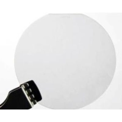
PAM-XIAMEN - Gallium Nitride Wafer Templates
PAM-XIAMEN’s Template Products consist of crystalline layers of (gallium nitride)GaN templates, (aluminum nitride)AlN template,(aluminum gallium nitride) AlGaN templates and (indium gallium nitride) InGaN templates, which are deposited on sapphire.
PAM-XIAMEN’s GaN Template consists of crystalline layers of gallium nitride (GaN), aluminum nitride (AlN), aluminum gallium nitride (AlGaN) and indium gallium nitride (InGaN), which are epilayer on sapphire and electronic grade for fabrication as MOS-based devices. PAM-XIAMEN’s Gallium Nitride Template Products enable 20-50% shorter epitaxy cycle times and higher quality epitaxial device layers, with better structural quality and higher thermal conductivity,which can improve devices in the cost, yield, and performance.
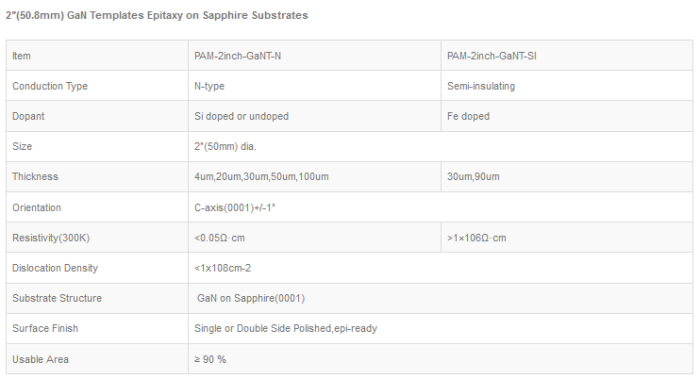
2″ (50.8mm)GaN Templates Epitaxy on Sapphire Substrates
- Item PAM-GaNT-P
- Conduction Type P-type
- Dopant Mg doped
- Size 2″(50mm) dia.
- Thickness 5um,20um,30um,50um,100um
- Orientation C-axis(0001)+/-1°
- Resistivity(300K) <1Ω·cm or custom
- Dopant Concentration 1E17(cm-3) or custom
- Substrate Structure GaN on Sapphire(0001)
- Surface Finish Single or Double Side Polished,epi-ready
- Usable Area ≥ 90 %
3″(76.2mm)GaN Templates Epitaxy on Sapphire Substrates
- Item PAM-3inch-GaNT-N
- Conduction Type N-type
- Dopant Si doped or undoped
- Exclusion Zone: 5mm from outer diameter
- Thickness: 20um,30um
- Dislocation density < 1x108cm-2
- Sheet resistance (300K): <0.05Ω·cm
- Substrate: sapphire
- Orientation : C-plane
- Sapphire thickness: 430um
- Polishing: Single side Polished,epi-ready, with atomic steps.
- Backside coating: (custom)high quality Titanium coating, thickness > 0.4 μm
- Packing: Individually packed under argon
- Atmosphere vacuum sealed in class 100 clean room.
3″(76.2mm)GaN Templates Epitaxy on Sapphire Substrates
- Item PAM-3inch-GaNT-SI
- Conduction Type Semi-insulating
- Dopant Fe Doped
- Exclusion Zone: 5mm from outer diameter
- Thickness: 20um,30um,90um(20um is the best)
- Dislocation density < 1x108cm-2
- Sheet resistance (300K): >106 ohm.cm
- Substrate: sapphire
- Orientation : C-plane
- Sapphire thickness: 430um
- Polishing: Single side Polished,epi-ready, with atomic steps.
- Backside coating: (custom)high quality Titanium coating, thickness > 0.4 μm
- Packing: Individually packed under argon Atmosphere vacuum sealed in class 100 clean room.
4″(100mm)GaN Templates Epitaxial on Sapphire Substrates
- Item PAM-4inch-GaNT-N
- Conduction Type N-type
- Dopant undoped
- Thickness: 4um
- Dislocation density < 1x108cm-2
- Sheet resistance (300K): <0.05Ω·cm
- Substrate: sapphire
- Orientation : C-plane
- Sapphire thickness: –
- Polishing: Single side Polished,epi-ready, with atomic steps.
- Packing: Individually packed under argon Atmosphere
- vacuum sealed in class 100 clean room.
2″ (50.8mm)AlGaN, InGaN, AlN Epitaxy on Sapphire Templates: custom
- 2”(50.8mm)AlN Epitaxy on Sapphire Templates
- Item PAM-AlNT-SI
- Conduction Type semi-insulating
- Diameter ? 50.8mm ± 1mm
- Thickness: 1000nm+/- 10%
- Substrate: sapphire
- Orientation : C-axis(0001)+/-1°
- Orientation Flat A-plane
- XRD FWHM of (0002) <200 arcsec.
- Useable Surface Area ≥90%
- Polishing: None
2”(50.8mm)InGaN Epitaxy on Sapphire Templates
- Item PAM-INGAN
- Conduction Type –
- Diameter ? 50.8mm ± 1mm
- Thickness: 100-200nm, custom
- Substrate: sapphire
- Orientation : C-axis(0001)+/-1O
- Dopant In
- Dislocation Density ~ 108 cm-2
- Useable Surface Area ≥90%
- Surface Finish Single or Double Side Polished,epi-ready
2”(50.8mm)AlGaN Epitaxy on Sapphire Templates
- Item PAM-AlNT-SI
- Conduction Type semi-insulating
- Diameter ? 50.8mm ± 1mm
- Thickness: 1000nm+/- 10%
- Substrate: sapphire
- Orientation : C-plane
- Orientation Flat A-plane
- XRD FWHM of (0002) <200 arcsec.
- Useable Surface Area ≥90%
- Polishing: None