Indeotec - Model PECVD -Mirror
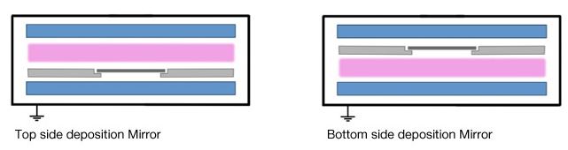
Plasma from top and beneath
Based on the IRFE design platform for the PECVD Classic reactor, our engineers went even further and introduced a 2nd electrode and a carrier plate with holes, thus enabling the double-sided plasma generation and hence, top and bottom deposition of the substrate. The height level at which the carrier plate is inserted into the reactor defines the deposition mode, either from the top or from the bottom-
This proprietary, truly innovative concept paves the way for numerous applications:
- Double-sided PECVD deposition of intrinsic and p/n doped a-Si:H layers for heterojunction PV cell devices
- Adaption of film deposition to slightly bended substrates (wafer bending)
- Customized thin film thickness profiles across the substrate surface without any change of plasma composition or stoichiometry
Excellent layer properties
Due to the reactor design, which allows an enhanced control of the plasma process, excellent layer properties will be obtained.
Examples for layers on wafer placed on hole carrier plates:
- Passivation > 10 ms (@ 5x1014 cm-3) for i-layer a-Si:H (4’’ FZ)
- Passivation > 5 ms (@ 5x1014 cm-3) for i/p-layer and i/n-layer (6’’ CZ)
Multiple layer deposition
Multiple layers (layer stacks) may be deposited in one reactor without any interruption of the vacuum.
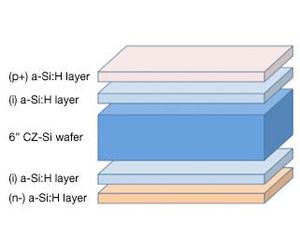
Example:
PECVD deposition of intrinsic and doped a-Si:H layers onto
Si wafers for the manufacture of hetero-junction PV cells.