

- Home
- Companies
- Enerpoint S.p.A.
- Products
- Photovoltaic Cell
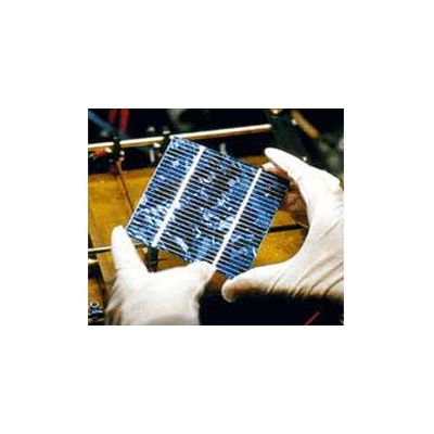
Photovoltaic Cell
The conversion of solar radiation into an electron current takes place in the photovoltaic cell, a device consisting of a thin sheet of semiconductor metal, very often made of suitably treated silicon.This treatment is characterised by various chemical processes including so-called `doping`.Adding impurities, that is atoms of boron and phosphorous, to the crystalline structure of the silicon generates an electrical field and produces the charges necessary for the formation of an electrical current. This is created when the cell, whose two faces are connected to a user, is exposed to the light.
The energy which can then be exploited depends on the characteristics of the material the cell is made of: conversion efficiency (the percentage of energy contained in the sunlight incident on the cell which is transformed into electrical energy by the photovoltaic device) for commercial silicon cells generally lies between 13% and 17%, while laboratory cells have produced a reading of 32.5%.
In practice, the typical photovoltaic cell has an overall thickness of between 0.25 and 0.35 mm and is made of mono or multi-crystalline silicon. Generally square, it has a surface measuring somewhere between 100 and 225 m² and, with an irradiation of 1 KW/m² at a temperature of 25°C, produces a current of between 3 and 4 A and a voltage of approximately 0.5V, generating 1.5-2 Wp of power.
The watt peak
As the power of a photovoltaic cell varies with changes in its temperature and radiation, standard parameters have been defined, producing the so-called watt peak (Wp) relating to the power supplied by the cell at a temperature of 25°C and a radiation of 1000 W/m², in AM1 conditions.
As well as crystalline type silicon, there has recently been a great deal of interest shown by various manufacturers in producing modules based on amorphous silicon. Actually, it is not strictly correct to refer to cells when talking about amorphous silicon, as it is generally deposited in layers on sometimes quite large surfaces.
As far as cost is concerned, traditional amorphous silicon costs less than (mono or multi) crystalline silicon, while the cost of amorphous silicon with two or three junctions should come down if it is to be used on a large scale.
he direct conversion of solar energy into electrical energy, achieved with photovoltaic cells, exploits the physical phenomenon of the interaction of light radiation with valence electrons in semiconductor materials. This is known as the photovoltaic effect. Whatever the material used, the mechanism by which the cell transforms sunlight into electrical energy is essentially unvarying. Let`s consider, for the sake of simplicity, the case of a conventional photovoltaic cell made of crystalline silicon.
Normally, the silicon atom has 14 electrons, four of which are in the valence band, and can therefore interact with other atoms, whether they are made of silicon or other elements. Two adjacent atoms belonging to a pure silicon crystal have a couple of electrons in common, one belonging to the considered atom, the other belonging to the adyacent one.
Therefore, there is a strong electrostatic bond between an electron and the two atoms which it helps to keep together. However, this bond may be severed by a sufficient amount of energy.If enough energy is supplied the electron is taken to a higher energy level (conduction band) where it is free to move around, thus contributing to the flow of electricity. When it moves into the conduction band the electron leaves a "hole" behind it, that is a lacuna where an electron is missing. A nearby electron may easily go and fill the hole, thus swapping places with it. To exploit the electricity it is necessary to create a constant movement of electrons (and of holes) , or rather a current, by means of an electrical field inside the cell. The field is produced by special physical and chemical treatments, creating a surplus of positively charged atoms in one part of the semiconductor and a surplus of negatively charged atoms in the other. In practice this condition is obtained by adding small quantities of boron atoms (positively charged) and phosphorous atoms (negatively charged) to the silicon lattice, or in other words doping the semiconductor. The electrostatic attraction between the two kinds of atom creates a fixed electrical field which gives the cell a structure known as "the diode structure", in which the transit of the current, consisting of mobile charge carriers, electrons for instance, is obstructed in one direction and facilitated in the opposite direction. The explanation of this phenomenon can be illustrated as follows.
In the layer doped with phosphorous, which has five valence electrons as opposed to the four in silicon, there is, for each atom of phosphorous, an extra unbonded electron, composed of an so-called valence electron that is free to move around.
In the layer doped with phosphorous, which has five valence electrons as opposed to the four in silicon, there is, for each atom of phosphorous, a weakly bonded negative charge, composed of a so-called valence electron.
Likewise, in the layer doped with boron, which has three outer electrons, there is a surplus positive charge, composed of the holes found in the boron atoms when they bond with silicon.
The first, negatively charged layer is labelled N, the second, positively charged layer is labelled P and the border separating them is called junction P-N.Putting the two layers opposite each other activates an electronic flow from zone N to zone P which, once it has reached the electrostatic point of equilibrium, determines a surplus of positive charge in zone N, due to phosphorous atoms lacking an electron, and an excess of negative charge in zone P, due to electrons migrating from zone N. The result is an electrical field within the device which separates surplus electrons, generated by the absorption of light, from the holes, pushing them in opposite directions (the electrons towards zone N and the holes towards zone P) so that an external circuit can collect the current thus generated.