- Home
- Companies
- Xiamen Powerway Advanced Material ...
- Products
- PAM-XIAMEN - Silicon Carbide Epitaxy ...
PAM-XIAMEN - Silicon Carbide Epitaxy (SIC)
We provide custom thin film (silicon carbide)SiC epitaxy on 6H or 4H substrates for the development of silicon carbide devices. SiC epi wafer is mainly used for Schottky diodes, metal-oxide semiconductor field-effect transistors, junction field effect
PAM-XIAMEN provide custom thin film (silicon carbide) SiC epitaxy on 6H or 4H substrates for the development of silicon carbide devices. SiC epi wafer is mainly used for Schottky diodes, metal-oxide semiconductor field-effect transistors, junction field effect transistors, bipolar junction transistors, thyristors, GTO, and insulated gate bipolar. With a silicon carbide wafer as a substrate, a chemical vapor deposition (CVD) method is usually used to deposit a layer of single crystal on the wafer to form an epitaxial wafer. Among them, SiC epitaxy are prepared by growing silicon carbide epitaxial layers on conductive silicon carbide substrates, which can be further fabricated into power devices.
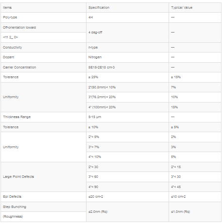
2 mm edge exclusion for 50.8 and 76.2 mm, 3 mm edge exclusion for 100.0 mmNotes:
- Average of all measurement points for thickness and carrier concentration (see pg. 5)
- N-type epi layers • Not all doping densities are available in all thicknesses
- Uniformity:standard deviation(σ)/average
- Any special requirement on the epi-parameter is on request
Introduction of SiC Epitaxy
Why do We Need Silicon Carbide Epitaxial Wafer? Because different from the traditional silicon power device manufacturing process, silicon carbide power devices cannot be directly fabricated on silicon carbide single crystal materials. High-quality epitaxial materials must be grown on conductive single crystal substrates, and various devices manufactured on the SiC epitaxial wafer.
The main epitaxial technology for SiC epitaxy growth is chemical vapor deposition (CVD), which realizes a certain thickness and doped silicon carbide epitaxial material through the growth of SiC epitaxy reactor step flow. With the improvement of silicon carbide power device manufacturing requirements and withstand voltage levels, SiC epi wafer continues to develop in the direction of low defects and thick epitaxy.
In recent years, the quality of thin silicon carbide epitaxial materials (
Since silicon carbide devices must be fabricated on epitaxial materials, basically all silicon carbide single crystal materials will be used as SiC epitaxial film to grow epitaxial materials. The technology of silicon carbide epitaxial materials has developed rapidly internationally, with the highest epitaxial thickness reaching more than 250 μm. Among them, the epitaxy technology of 20 μm and below has a high maturity. The surface defect density has been reduced to less than 1/cm2, and the dislocation density has been reduced from 105/cm2 to 103/cm2. The dislocation conversion rate of base plane is close to 100%, which has basically met the requirements of epitaxial materials for large-scale production of silicon carbide devices.
In recent years, the international 30 μm~50 μm epitaxial material technology has also matured rapidly, but due to the limitation of SiC epi market demand, the progress of industrialization has been slow. At present, industrialization company can offer silicon carbide epitaxial materials in batches, include Cree SiC epitaxy, PAM-XIAMEN SiC epitaxy, Dow Corning SiC epitaxy etc..
Test Methods
- No.1. Carrier concentration:Net doping is determined as an average value across the afer using Hg probe CV.
- No.2. Thickness: Thickness is determined as an average value across the wafer using FTIR.
- No.3.Large point defects: Microscopic inspection performed at 100X, on an Olympus Optical Microscope, or comparable.
- No.4. Epi Defects Inspection or defect map performed under KLA-Tencor Candela CS20 Optical Surface Analyzer or SICA.
- No.5. Step bunching: Step bunching and Roughness are scaned by AFM (atomic force microscope) on a 10μm x10μm area
Large Point Defects Descriptions
Defects which exhibit a clear shape to the unassisted eye and are > 50microns across. These features include spikes, adherent particles, chips andcraters. Large point defects less than 3 mm apart count as one defect.
Epitaxy Defect Descriptions
SiC epitaxy defects include 3C inclusions, comet tails, carrots, particles, silicon droplets and downfall.
- Power factor correction(PFC)
- PV inverter and UPS(Uninterrupted power supplies) inverters
- Motor drives
- Output rectification
- Hybrid or electric vehicles
- SiC Schottky diode with 600V, 650V, 1200V, 1700V, 3300V is available.