
- Home
- Companies
- VIEW Micro Metrology
- Applications
- VIEW Semiconductor Advanced Packaging ...
VIEW Semiconductor Advanced Packaging Applications - Fan-out Wafer Level Packaging - Electronics and Computers - Semiconductors
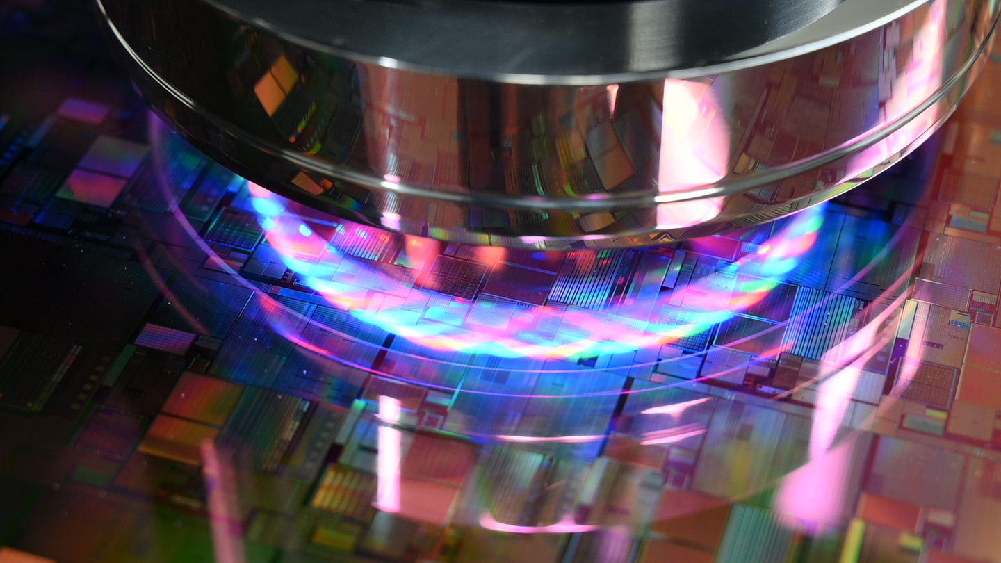
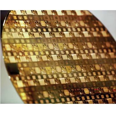
Accurate metrology is needed in FOWLP to inspect wafer warpage, die position/alignments, flatness/coplanarity, through-silicon vias, solder microbump heights, UBM layers, RDL lines, and other alignments and features. VIEW Micro Metrology systems and software are ideal for this type of work by providing high-accuracy measurement, high-throughput speed, and production line integration.
As the leader in microelectronics metrology solutions for more than two decades, VIEW brings together the applications awareness and metrology expertise needed to address even the most demanding interconnection challenges with proven platforms. Some of the specific microelectronics interconnection applications that are addressed by VIEW solutions are listed below.