
VIEW Micro Metrology applications
Accurate metrology is needed in FOWLP to inspect wafer warpage, die position/alignments, flatness/coplanarity, through-silicon vias, solder microbump heights, UBM layers, RDL lines, and other alignments and features. VIEW Micro Metrology systems and software are ideal for this type of work by providing high-accuracy measurement, high-throughput speed, and production line integration.
Flip chip processes present a number of critical metrology challenges including the need for precise three-dimensional measurements to accurately inspect pad size, position, and distance from the package edges as well as confirming acceptable flatness and coplanarity.
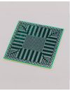
Measure a wide variety of critical dimensions on MEMS devices, including pitch, width, and spacing of flexures, fingers, combs, arcs, circle diameters, and center locations. Because of the myriad of requirements for MEMS devices, they can range from a few microns in size to a few millimeters.
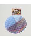
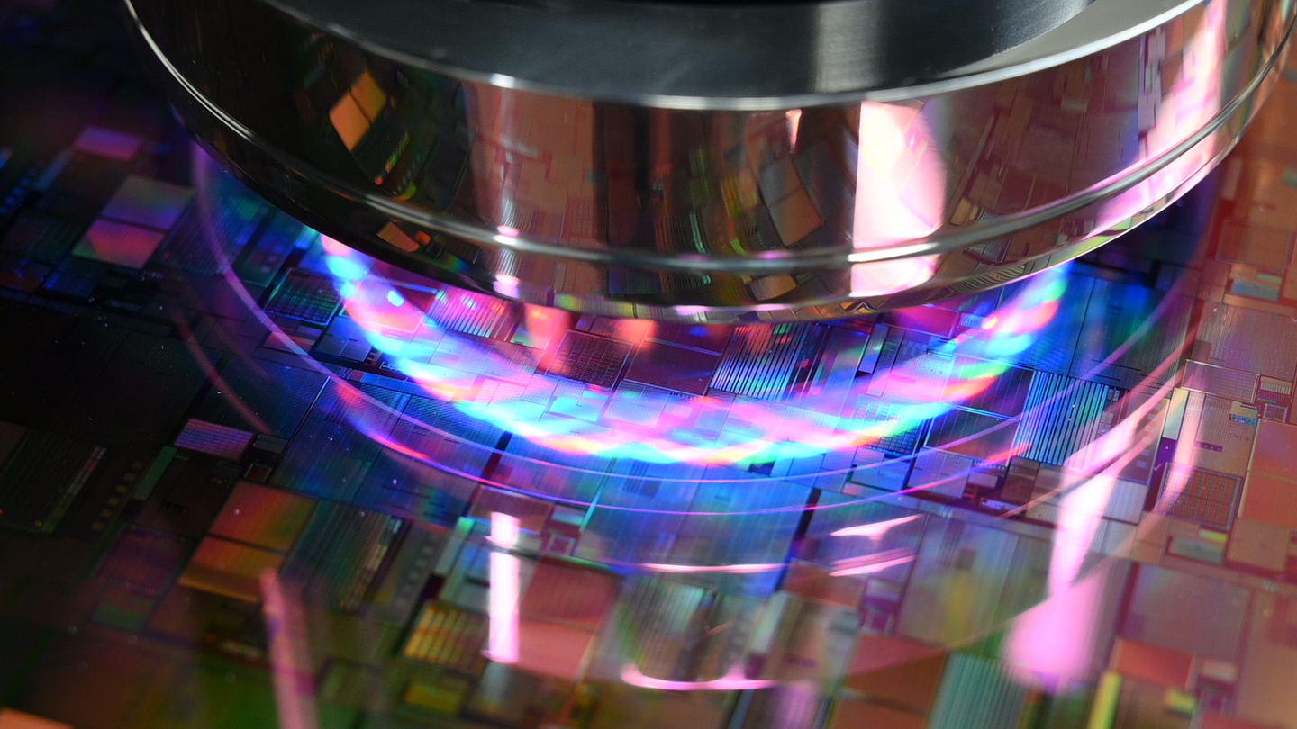
As today’s semiconductor designs continually become smaller and denser, the challenges of wafer inspection are constantly escalating. Extremely small feature sizes can require 50X or higher objective lens magnification and highly programmable top-lighting/back-lighting, along with ultra high-resolution accuracy and repeatability.
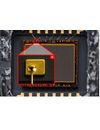
The small features, fragile connections, and critical three-dimensionality of wire bonded assemblies require high-performance, non-contact metrology solutions. Functions such as multiple magnification, creative lighting, and advanced image processing are needed in order to measure critical features such as ball and tooling mark diameters, placement and pad alignment, and wire loop height.
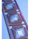
Leadframe inspection presents a wide variety of feature sizes and geometry, requiring metrology systems that can be flexibly programmed for fast and accurate three-dimensional measurements. Die-to-pad placement/alignment, lead positions/sizes, lead tilt and twist angles, pitch, lead widths, lead-coplanarity, and dam-bar dimensions all represent critical factors that must be tightly controlled.
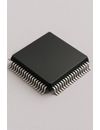
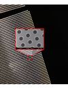
Quad Flat Pack (QFP) and Ball Grid Array (BGA) components represent metrology challenges with very tight tolerances that can tax the capabilities of even high performance systems.
Precision stencils for SMT solder paste printing represent a critical linchpin in the achievement of overall productivity and quality manufacturing results within the electronics industry. High-end metrology systems play a vital role in the assurance of the stencil quality needed for producing consistent production results.