
- Home
- Companies
- VIEW Micro Metrology
- Applications
- VIEW Semiconductor Advanced Packaging ...
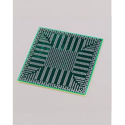
VIEW Semiconductor Advanced Packaging Applications - Flip Chip - Electronics and Computers - Semiconductors
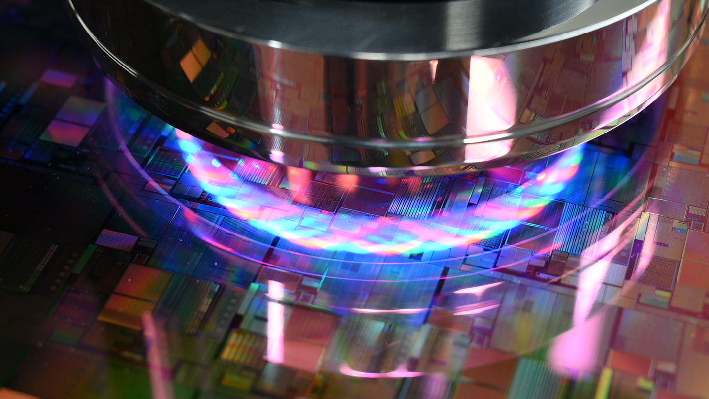
Flip chip processes present a number of critical metrology challenges including the need for precise three-dimensional measurements to accurately inspect pad size, position, and distance from the package edges as well as confirming acceptable flatness and coplanarity.
Most popular related searches
Accurate and efficient non-contact inspection of flip chips often requires advanced features such as multiple levels of magnification, Programmable Ring Light (PRL), and integrated lasers to improve inspection throughput rates.
Stay in the loop!
Select your areas of interest to receive industry updates.