

- Home
- Companies
- SENTECH Instruments GmbH
- Products
- SENTECH - Model SI 500 - ICP-RIE Plasma ...
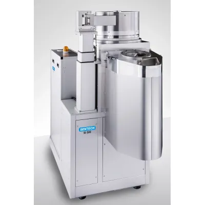
SENTECH - Model SI 500 -ICP-RIE Plasma Etch System
The SENTECH SI 500 ICP-RIE System represents advanced inductively coupled plasma reactive ion etching technology, tailored for both research and industrial applications. Its core feature, the proprietary Planar Triple Spiral Antenna (PTSA) plasma source, offers uniform plasma generation with high ion density and low ion energy, making it ideal for low-damage etching of sensors, quantum dots, and HEMT. The system supports high-rate plasma etching of silicon for MEMS with high aspect ratios using room temperature and cryogenic processes. Dynamic temperature control, achieved through a sophisticated substrate electrode combined with He backside cooling and precise backside temperature sensing, ensures optimal process stability across a wide temperature range. This versatility allows the SI 500 to handle a multitude of materials, including compound semiconductors (GaAs, InP), dielectrics, and metals. The modular design accommodates a variety of substrate sizes and configurations, from single wafer vacuum load locks to complex cluster tools, enabling high flexibility and throughput. Advanced control is provided by a reliable PLC and SIA operating software, supporting robust real-time system management.