

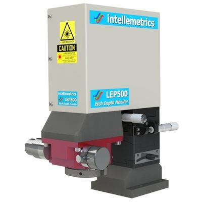
Intellemetrics - Model LEP500 -Real-time Plasma Etch Depth Monitoring System
The LEP500 is a specialized system designed for real-time, in-situ monitoring and endpoint detection within plasma etch processes. It is geared towards enhancing precision in semiconductor, optoelectronics, MEMS, and thin film removal applications by providing accurate etch depth and rate data. The system can be swiftly integrated into most modern plasma etch machines via a clear normal incidence view port, often found in the center of the top electrode. It offers robust process control solutions by reducing noise interference and minimizing setup costs in both production and R&D environments. Equipped with EtchDirector software, it enables real-time calculation and control of etch parameters, thereby optimizing process termination. The LEP500 can function as both a standalone unit and an integrated part of OEM etch tools, supporting a straightforward communication interface.
Real-time, in-situ plasma etch depth monitoring and end point detection plus co-linear wafer vision system.
If the plasma etch depth of your device is important, then you need the LEP500. Hit your target etch depth first time and every time.
Within minutes the LEP500 can be fitted to just about any plasma etch machine that has a clear normal incidence view of the wafer being etched. This is usually through a small window port in the centre of the top electrode. Most modern etch machines come with such a central window as standard and most manufacturers will supply a modified electrode upon request. If you have any doubts about your particular plasma etch tool then feel free to contact us for advice.
The LEP500 plasma etch depth monitors provide real-time process control solutions for a wide range of dry etch applications including semiconductors, optoelectronics, MEMS, failure analysis and general thin film removal.
The instrument offers in-situ monitoring solutions with excellent noise rejection and reduced set-up costs for both production and R&D environments. The system includes a user-friendly Windows-based environment for input, control and visualisation. EtchDirector software calculates the etch rate and etch depth in real time enabling enhanced control of process termination.
The LEP500 is designed to operate either as a standalone tool, or to be integrated into an OEM etch tool through a simple and robust communications interface.
The LEP500 Series comes in a number of different configurations to satisfy the etching needs of a wide range of diverse materials as well as the diverse needs of a wide range of applications – from flexible research and development labs to the stringent requirements of high volume production facilities. We have made the range as modular as possible to enable you to choose the system that meets your specific requirements.
- Monitoring Wavelength :670nm, 980m or 1550nm
- Working Distance :200mm to 800mm wafer to LEP500
- Camera Image :5 Mpixel
- Image Resolution :Working Distance dependant. 4um to 10um
- Laser Spot Size at Wafer :Working Distance dependant. 8um to 40um at FWHM
- Collimation :Built-in 2-axis goniometers
- Alignment :Built-in X-Y Stages
- Manual or Motorised stages
- Motorised stages controlled via remote joystick, or via software commands
- Operation :Either Manual or integrated into etch chamber control system for fully automated operation
- Coms Interface :Digi IO and/or TCP/IP
- Controller Module :2U x 19inch rack mount ruggedised controller module running under Win 10 Pro, with all software and interfaces
- Software :Full EtchDirector software suite
Materials
- III-V
- II-VI
- Silicon
- Polymers
- Dielectrics
- Metals
Product Sectors
- Optoelectronics: lasers, modulators, detectors
- Silicon: CMOS, trench isolation, wafer thinning, vias
- MEMS: buried oxide etch, deep silicon etc
- Photomask: metals & dielectric etch
- Packaging: topographic surfaces
- Bio Chips: micro-channel etch
- Failure Analysis
GaAs/AlGaAs Quantum Cascade Laser Etch
Over 200 layers were modelled using EtchDirector’s modelling capability as shown in the left-hand window.
The right-hand window shows the results from the actual etch run. The LEP500 reproduced the modelled data to a high degree and detected each turning point during the run enabling the progress of the etch to be followed and for the process to endpoint with a high degree of accuracy.
The LEP500’s combination of modelling and monitoring capability removed the need for 4-5 ‘vent-&-measure’ steps or performance of numerous sacrificial calibration runs, saving significant time and expensive epi-wafers.
The level of certainty achievable with the LEP500 becomes even more critical for devices requiring multiple etch stages.
The achievable etch stop accuracy in this case was around 5nm.
Failure Analysis Etch: SiO2 on Aluminium
As the graph above indicates, the LEP500 can be used to monitor the etch back of dielectric on metal for a number of applications including failure analysis.
The LEP500 monitors a small (approx 20 micron diameter) exposed area and is therefore ideal for monitoring one small chip in an entire chamber – unlike optical emission spectroscopy which would struggle to detect such dilute species.
EtchDirector utilises an advanced end point algorithm to detect the ‘flat-line’ at the end of the oxide etch. In field tests, EtchDirector reliably detects the endpoint well before a skilled operator, thereby avoiding unwanted removal, damage or contamination of the underlying Al layer. The endpoint algorithm also allows the user to enter an overetch time to enable full clearout across the wafer.
A major advantage of this algorithm is that reliable endpointing does not depend upon the starting oxide thickness. This is especially important in a manufacturing environment where pre-measurement of the oxide thickness is prohibitive in terms of time and cost.
The LEP500 is also ideal for monitoring the etch of SiN on metal or even combinations of SiN on SiO2 or on Si.
Metal Etching
Metals are not transparent until very thin and therefore you cannot obtain interference fringes and monitor etch depth & rate through the bulk of a metal layer.
However, the LEP500 is ideal for picking out interfaces, indicated by a step level change in reflectivity. The above example shows titanium being etched from a LiNbO3 substrate. Whilst monitoring at 670nm, the large drop in signal occurs over an etch depth of less than 30nm. EtchDirector comes with an endpoint algorithm specifically designed to identify this step level change and enables the operator to choose whether to stop at the top, middle or bottom of the curve. Again, an overetch capability is also included to enable a clearout etch to be achieved.
A major advantage of this algorithm is that reliable endpointing does not depend upon the starting metal thickness. This is especially important in a manufacturing environment where premeasurement of the metal thickness is prohibitive in terms of time and cost.
This process works even at high etch rates and has been proven to be faster and more accurate than a skilled operator. The process works equally well for other metals including NiCr, Ni, Au, Tg, Pt, etc, and works for a wide range of substrates.